

The move to TSMC and custom silicon
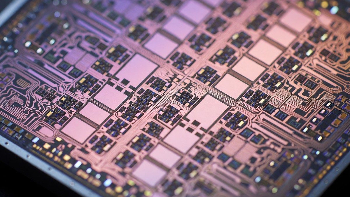
Google uses TSMC 3nm manufacturing for the Tensor G5, marking a departure from Samsung Foundry. This transition reduces voltage leakage by 27% compared to Samsung 4nm. Google also designs more custom components now. It uses a Faraday Technologies FTPWMTMR010 PWM controller and a VeriSilicon DC9000 display controller instead of Samsung parts. The new custom image-signal processor processes light data to improve camera performance. This structural shift allows Google to fix hardware bugs that previously caused heat issues. I see this move as a way to gain better control over the device experience. Google’s decision to work with TSMC stems from the Taiwanese company’s reliability with advanced nodes. The Tensor G5 also uses Synopsys DesignWare IP cores for USB3 and MIPI interfaces. The chip pairs with 16GB of LPDDR5X memory and a 4,700-mAh battery. This hardware supports a 50MP primary camera and a 6.3-inch Actua OLED panel with 2,000-nits peak brightness.
Performance trade-offs and competition
The Snapdragon 8 Elite beats the Tensor G5 in almost every benchmark. The Qualcomm chip hits 3126K on AnTuTu while the Google chip reaches 1549K. The Snapdragon 8 Elite also shows 24% higher memory bandwidth at 84.8 GB/s compared to the 68.2 GB/s available on the Tensor G5, while also reaching a much higher CPU clock speed of 4320 MHz and greater memory capacity. During my tests, the Tensor G5 CPU temperature stayed at 45C, which is lower than the 61C on the Snapdragon 8 Elite. However, the Tensor G5 throttled to 47% of its peak output during heavy loads. The Snapdragon 8 Elite only dropped to 81% of its maximum output.
| Metric | Snapdragon 8 Elite | Tensor G5 |
|---|---|---|
| AnTuTu Score | 3126K | 1549K |
| Memory Bandwidth | 84.8 GB/s | 68.2 GB/s |
| CPU Clock Speed | 4320 MHz | 3780 MHz |
| CPU Temperature | 61C | 45C |
| Throttling | 81% | 47% |
The Snapdragon 8 Elite also produces 3379.2 Gigaflops of GPU power, while the Tensor G5 produces 1689.6 Gigaflops. I find the Tensor G5 performs better for daily tasks like web browsing and app launches. The G5 delivers 25% faster web browsing and 15% faster app launches compared to previous models. The Snapdragon 8 Elite supports 8K video at 60FPS and 4K at 120FPS, while the Tensor G5 supports 8K at 30FPS and 4K at 120FPS. The Qualcomm chip also reaches 10,000 Mbps download speeds with the Snapdragon X80 modem.
AI latency and future hardware
On-device AI remains a focus for the Tensor G5 through its upgraded NPU. The chip delivers Gemini Live responses in under 800ms. This local processing protects user privacy because it avoids cloud servers. Most users, however, care more about battery and heat than AI. One survey found 81.4% of owners want better thermal management and battery capacity. A survey of more than 1,700 readers found 69.2% wanted Google to cancel the Tensor line entirely. I would suggest focusing on the 3nm efficiency if you record long videos. You should consider if the 3nm efficiency helps your specific workflow before you buy. The upcoming Tensor G6 rumors suggest a 2nm process and 50% more TPU compute. The G6 might also offer AI tasks that run 3.5x faster while using 3.5x less energy. Will the 2nm process in the next generation finally stop the performance dips during gaming?