
Design methodology and leadership
Richard Yu, CEO of Huawei Consumer Business Group, directs the company’s focus toward devices, connectivity, cloud computing, and chipsets to power an AI "Superphone." This vision requires a new information-management architecture to handle information explosion. He Tingbo, president of Huawei’s semiconductors business department, leads the technical implementation through the Tau Scaling law. She introduced this law at the 2026 IEEE International Symposium on Circuits and Systems to replace geometric scaling with time scaling. This approach uses LogicFolding, a design architecture that expands from a single-layer to a double-layer architecture to improve transistor density. Huawei aims to move from local critical-path folding to full-scale and multi-layer folding between 2026 and 2035. You already know how US export controls complicate these designs. The company builds an ecosystem with partners like MiniMax and iFLYTEK to demonstrate its "All Intelligence" strategy. Rotating Chairman David Wang and the heads of the ICT Business Group and Huawei Cloud, Yang Chaobin and Dr. Peter Zhou, set the strategic direction for this strategy. The third World Internet Conference in Wuzhen featured speeches by Chinese President Xi Jinping and Liu Yunshan, who delivered the opening remarks.
Manufacturing and the SMIC production gap
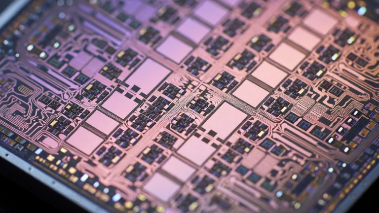
SMIC produces the Kirin 9030 using its third-generation 7nm (N+3) process, which reaches a minimum metal pitch of 32.5 nm. This density matches TSMC N6 through aggressive DUV multi-patterning, but the method increases complexity and production expenses. The 7nm process for Huawei’s Ascend 910B chips reports yields between 20% and 40%, which falls far below industry standards. Because SMIC cannot access EUV lithography, the company must use DUV machines three to four times to produce a single 7nm chip, which increases both energy consumption and maintenance costs for the manufacturer. While the Kirin 9030 improves middle core performance by 17% over the 9020, it still trails flagship SoCs from Apple and Qualcomm. The Kirin 9030 includes a 20% increase in the shared L3 cache for the big cluster. The prime core is a 10% frequency increase from 2.5 GHz to 2.75 GHz. The GPU in the Kirin 9030 is 10% larger in area, and the number of compute units is 6 instead of 4. SMIC also works with Alibaba Group to develop 5nm chips for AI inference workloads. To fund these efforts, SMIC uses state-directed investments, such as the 344 billion yuan ($47.5 billion) national semiconductor fund. The company also moved to acquire full control of its Beijing subsidiary, Semiconductor Manufacturing North China, for $5.79 billion in January 2026.
The Mate 70 hardware specifications
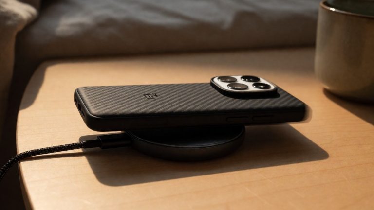
The Mate 70 Air is a slim phone with a 6.6mm thickness and a 208g weight. It contains a 6500mAh battery, which is much larger than the 3149mAh capacity in the iPhone Air. The device uses Kunlun Glass for the front and is IP68 and IP69 rated for dust and water resistance. The Kirin 9020A chipset powers the 16GB RAM variant, while the 12GB model uses the Kirin 9020B SoC. The 7-inch Full-HD+ AMOLED display has a 2760 x 1320 resolution and a 300Hz touch sampling rate. The quad rear camera system includes a 50MP primary sensor, a 12MP telephoto lens, an 8MP ultrawide camera, and a 1.5MP multi-spectral color sensor. The Mate 70 Pro Plus, released in November 2024, has 16GB of RAM compared to the 8GB in the Apple iPhone 16 Pro Max. This Pro Plus model has a 5700mAh battery, which is more than the 4685mAh capacity of the iPhone 16 Pro Max. The Mate 70 Air starts at CNY 4,199 for the 12GB variant.
| Feature | Huawei Mate 70 Air | iPhone Air |
|---|---|---|
| Thickness | 6.6 mm | 5.6 mm |
| Weight | 208 g | – |
| Battery | 6500 mAh | 3149 mAh |
| Display | 7-inch AMOLED | – |
| Resolution | 2760 x 1320 | – |
| RAM (Max) | 16 GB | 8 GB |