
AMD MI350X versus Nvidia Blackwell
AMD released the Instinct MI350 series to challenge Nvidia’s Blackwell processors. The MI350X uses the CDNA 4 architecture and carries 288GB of HBM3E memory. This capacity exceeds the 192GB found in the Nvidia Blackwell B200. The MI355X variant provides 10% more FP6 performance than the base MI350X. This new series delivers four times the AI compute performance and 35 times the inferencing capabilities of the previous generation. AMD also introduced the AMD Developer Cloud to give developers access to MI300 and MI350 GPUs via cloud infrastructure. This service follows the launch of Nvidia DGX Cloud Lepton last month. AMD expects an $800 million hit from export controls on chips for China, while Nvidia expects a $4.5 billion write-down from the same restrictions. AMD’s stock fell roughly 24% in the past 12 months, whereas Nvidia’s stock rose more than 19% in the same period. AMD targets a competitive position through the MI325X, which challenges the Nvidia H200. MI350 systems with up to 64 GPUs use air cooling, while systems with 128 GPUs use liquid cooling.
Memory and compute comparison
The memory capacity advantage of AMD benefits large language model inference. The MI350X carries 288GB of HBM3E memory with 8TB/s of bandwidth. This capacity allows the chip to host 520B parameter AI models with ease. The B200 provides 192GB of memory, but Nvidia’s GB200 superchip pairs two Blackwell GPUs to provide 384GB of memory. The MI355X platform, which contains 128 GPUs and 36TB of HBM3e memory, delivers a peak throughput of 2.6 exaflops at FP4 precision for intense, large-scale data center workloads. You should focus on the memory-to-compute ratio when evaluating these two architectures.
| Specification | AMD MI350X | Nvidia B200 |
|---|---|---|
| Memory Capacity | 288GB HBM3E | 192GB HBM3E |
| Memory Bandwidth | 8TB/s | Not specified |
| FP4 Performance | 10 PFLOPS (MI355X) | 20 PFLOPS |
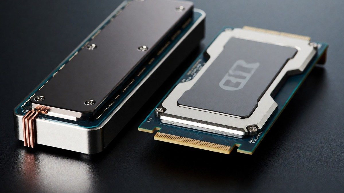
AMD claims the MI355X provides 40% more tokens-per-dollar cost efficiency than the B200. This efficiency makes the MI350 series a value-oriented choice for inference. The MI350X is an OAM module, whereas the B200 uses an SXM module. AMD claims the MI350X delivers 2.6 times the inference throughput of an H100 on Llama 3.1 405B. The B200 can serve the GPT-OSS-120B model for as little as $0.02 per million tokens. A 96-GPU version of the MI355X exists with 27TB of HBM3e memory.
Yield issues and training speed
Nvidia faces production hurdles with its Blackwell family. The B200 uses TSMC’s CoWoS-L technology, which requires complex packaging of multiple dies. Supply chain reports indicate that B200 yields remain between 90% and 95%, failing to meet internal TSMC standards. This technical difficulty causes shipment delays and forces Nvidia to focus on GB200 NVL72 systems. The B200 is a monolithic chip containing 208 billion transistors. The newer B300 variant provides enhanced memory subsystems and supports the Rubin-era networking stack. The GB300 NVL72 delivers 1.5 times the AI performance of the original GB200 NVL72, and Nvidia is also planning the Rubin system for 2026, which will include 576 GPUs and 15 exaflops of FP4 inference.
Performance benchmarks show a gap in training speed. In MLPerf Training v4.1, a DGX GB200 NVL72 cluster trained GPT-3 175B in 3.1 minutes. An 8-GPU MI350X node trained the same model in 4.8 minutes, though AMD’s MI350X produces lower total system costs and uses less power during these training runs. Will the MI400 launch in 2026 bridge this performance gap? The MI400 will carry 432GB of HBM4 memory and 19.6TB/s of bandwidth. The MI400 also plans to deliver 10x more performance for Mixture of Experts models when paired with future EPYC Venice CPUs and Vulcano NICs. AMD aims to increase rack-scale energy efficiency by 20x compared with 2024 by 2030.